Yeah I am still a little pissed that the competition is still around and we aren’t, and by "we" I mean Commodore Business Machines (CBM). It was Commodore that had the most popular home computer ever in the C64 (27 Million) and it was a team of MOS engineers after all, that had the idea to make a "micro" processor out of a 12 square inch PCB.
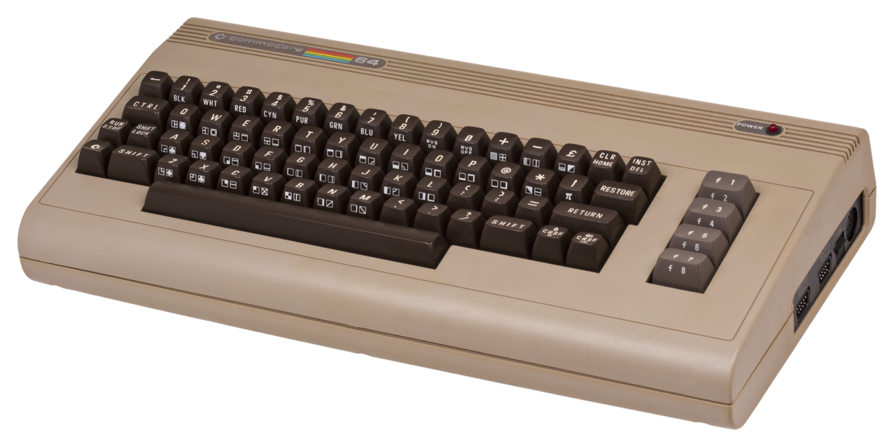
MOS Technology in King of Prussia/Norristown
Of course they did work at Motorola at the time and “Mot” did not want anything to do with a reduction of the profit margin on the pie-plate size processor. Of course MOS got sued by Motorola but that was an average Tuesday at MOS/CBM. I absolutely credit CBM with buying the MOS Technologies chip foundry, as together we could make our own processors, graphics chips, sound chips, memory controllers, and programmable logic.
With this arsenal at our call we didn’t have to make compromises the way other companies did such as conforming to the bus spec of an industrial standard 6845 or having to add extra logic when a custom extra pin would work. We could also make sprites.
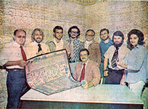
6502 Design Team (EE Times 1975, archive.archaeology.org)
The compromise we did have to make when designing was cost, and I mean the kind of cost reduction where finding a way to save a dollar ($1USD) saved millions in the production run. I knocked $.90USD out of a transformer one day and I couldn’t focus the rest of the day due to elation.
Cost reduction is a harsh mistress however as you can't just do it a little some of the time or only when you want to. The mental exercise of multiplying anything times a million was always there, it made it hard to buy lunch — I’d be blocking the lunch line while figuring the cost of a million tuna sandwiches FOB Tokyo
To offset stringent cost control we had massive quantity discounts. Calling a local rep to say that we were designing in the recent 16kx4 DRAM was known as "the call", and inevitably the doorbell would ring 2 minutes after hanging up the phone.
In a rare event we lost our management when [Mr. Jack Tramiel] quit and then later ended up at Atari — picture the Borg knowing everything Cpt. Picard does. During the time of "no management" a couple of things happened: the number of cases of beer consumed on premises skyrocketed, and the engineering department designed a computer to fill the void without direction from management or marketing, at least for a while.
This meant that the design ultimately came from a piece of grid paper instead of a few dozen meetings discussing customer focus and the cost of a million tuna sandwiches. The shopping list included a memory manager and the biggest PLA we had done to date. It should be noted that no one in chip design says "no" or "we can't do it" at this stage. That’s because we just don't yet know. But if the engineer making the requests doesn’t want to later be done in by the laws of physics, he/she had better keep the requests within the realm of "almost doable".
In the Commodore 64 there was a PLA modeled after the Signetics 82S100 which was a "blown fuse" technology for programming a simple AND-OR array. When I say blown fuse I am not kidding, my memory is that part of the parameters was not to blow the fuse using excessive power as it my "splatter".
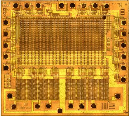
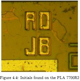
PLA Die C128.com,
Ultimately Commodore and MOS Technologies made their own NMOS version, I won't say we copied the Signetics part, we just took lots of Polaroids through a microscope and had them mounted to a board. Under the covers we replaced two kinds of fuses, "and term" fuses and "or term", with a diffusion layer "slug" and also a pre-ohmic contact. It was one-to-one so the code that worked on an 82S100 could be sent over and then someone could run a script to convert. An excellent write up on Commodore's C64 PLA down by [Thomas 'skoe' Giesel] embodied in this PDF (also mirrored here).
 The PLA is an AND-OR array meaning that each line of terms that are true — they satisfy the logic of “This and That but Not That over there” — are OR'ed together depending on which output you want to affect. OR’ing is like a dogpile, the chip doesn’t care which of the strings of terms caused the true condition, it just knows that one or more did.
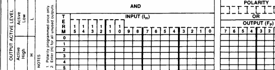
Example of the worksheet engineers used to create logic terms.
We pushed this device for everything it was worth, I had asked for a little over twice the terms which means the array, being twice as big, had twice the resistance and twice the capacitance. This translates to 4 times the RC component. That aside and I also won't bore with details of how the designer tried to insert a change without telling anybody and shorted all of the input pins to the back bias ring with 2 weeks to go to CES. Simply put we shoved as much into the chip as we could and we wouldn't have had a viable computer without it. Mass quantity production pricing brought the cost down to pennies and nickels, even after the $2.5million NRE cost to design.
PLA And Or Array
So the PLA was a low cost, high return hit. We smiled. Then we looked at what we call the jungle logic left on the board and our brows furrowed. This collection of gates would be prime candidates for the Programmable Logic Device (PLD) of the day, especially in the area where we were trying to make a 6502 microprocessor play nice with a Z80 microprocessor all while not blowing the DRAM up. It would also have been ideal for the final stages of FCC application where you can only make minimal visible changes to the board without re-submitting. There was no joy in Mudville however, as the price of PLDs was prohibitive at $4-$5USD. Buying large quantities didn’t result in large discounts, just large bills and logistics issues such as programming them. At this point I got my hands on a confidential stock and price sheet and picked the jungle logic from what was already in stock providing there were hundreds of thousands available of any one part.
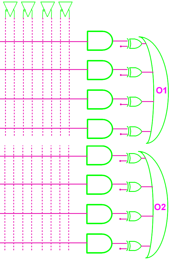
PLD architecture showing registers and feedback.
What made the PLA powerful was it was relatively fast since the internal array was small, and there was the addition of registers and feedback terms which are the ingredients of State machines (we will discuss Mealy and Moore state machines at a later date.) I believe CBM/MOS did try to do an NMOS version of the PLA but the limitations of the NMOS process limited usability. In the next installment — which will be published early tomorrow — I talk about more modern Complex Programmable Logic Devices and program one from start to finish. Instead of doing gate reduction, the modern devices quite simply allow a designer to implement macro functions at any quantity that simple couldn’t be done otherwise as "jungle logic" would be too slow and error prone.
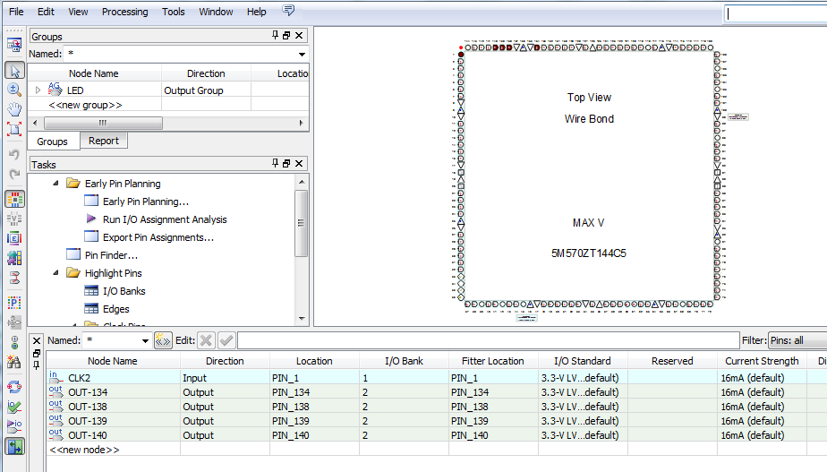
CPLD Device showing assignments.
Filed under: classic hacks, Featured
